 Slashdot Mirror
Domain: wikichip.org
Stories and comments across the archive that link to wikichip.org.
Comments · 17
-
Re:Mind-bending
Given that the diameter of a silicon atom is around 0.2nm, that means they are now building transistors out of something like 30-35 atoms across
Not even close. First, the silicon cubic lattice side is 0.543 nm, the atomic spacing is roughly 1/3 to 1/2 of that. When counting atoms, that's what you use, not atomic radius (which you seem to have misquoted as diameter.) Second, the gate pitch for TSMC's 7nm is 54 nm So each transistor covers an area something like 100-150 atoms on a side on the very crude assumption that the transistor is square, or about 10K to 40K atoms.
Somebody who actually does this for a living, please check my numbers.
-
Re:They better be optomistic.
It's an outright fact that intel measures their foundry processes FAR closer to real figures than the others
What real figures? There is no 14nm dimension in Intel's 14nm node either. Intel's node name may be more conservative than TSMC's, but nothing makes it "real". You are just blowing smoke out your ass.
-
Re:Abandon it
The article you linked compares Intel to Global Foundries, which doesn't even have a 7nm process as of today. You're still right, but try my links
Note that Samsung also went for 36nm minimum metal pitch and for what it's worth, also seem to be behind TSMC by about the same lag as Intel. It's starting to look like TSMC went for exactly the right amount of conservative.
I think that Intel is behind by exactly as much as I think
-
Re:Abandon it
The article you linked compares Intel to Global Foundries, which doesn't even have a 7nm process as of today. You're still right, but try my links
Note that Samsung also went for 36nm minimum metal pitch and for what it's worth, also seem to be behind TSMC by about the same lag as Intel. It's starting to look like TSMC went for exactly the right amount of conservative.
I think that Intel is behind by exactly as much as I think
-
Re:Quality journalism?
Correction: Intel's 10nm minimum metal pitch is only 10% smaller than TSMC's 7nm, not 22% as I wrote above. That is still enough to explain why Intel is having much worse problems than TSMC at the extreme limit of what deep UV can do.
-
Quality journalism?
Two days before AMD reports, three days before Intel reports, Semiaccurate floats this rumor with pretty much nothing to back it up. Here's the meat of their argument Note: The following is analysis for professional level subscribers only. So this is about signing up subscribers? Or an attempt at illegal stock manipulation? Both? It is certainly not about quality journalism.
I am definitely an AMD fanboy, full disclosure there. But that doesn't make me an Intel hater, at least not when they lay off the dirty tricks, which appears to pretty much the situation at the moment. So... balanced assessment: no reason to doubt Intel's revised 10nm production schedule. This is all about yields as Semiaccurate is fond of pointing out.
You can see from this that Intel's 10nm fin pitch is a bit more aggressive than TSMC's 7nm, 6% smaller. Intel's minimum metal pitch is a lot more aggressive, 22%. This is all right at the limit of what deep UV alone can do, so that might be Intel's bridge too far right there. I have a whole lot of difficultly believing that Intel did not learn enough from their aborted ramp up last spring to know exactly what they need to do to hit their yields, most probably including respinning their masks to a density nearly identical to TSMC.
Buried in there somewhere I did find one credible little nugget... Semiaccurate pointed out that last spring's 8121U Cannon Lake part, produced in limited quantities and only ever seen in the hands of a few reviewers, is specced without a GPU. Not because it doesn't have one, but because does have one but it doesn't work. I find that credible. Debugging both a processor and a GPU is much more work that just a processor or GPU alone. In contrast, AMD doesn't try to fab APUs until both the processor and GPU have been successfully fabbed separately. Excellent strategy, a big risk reduction.
Another huge thing AMD did to cut the 7nm risk was, jumping into bed with the phone industry. Intel convinced themselves it was a good idea to go it alone as usual, and were proved colossally wrong. Though I am not going to claim any special inside information, I think that Intel is going to bring up its Cannon Lake production successfully, 3 or 4 years behind schedule as they say, and that this is the end of the line for Intel as an independent fab. It's simple: the days of always being a node ahead are over, today they are half a node behind. From here on, there are no advantages to running an independent fab, only disadvantages. When Intel finally does ramp up Cannon Lake they will be in an excellent position to negotiate a new, cooperative deal with the rest of the industry, but if they persist in marching to their own drumbeat they will pay an enormous cost in market share and operating income over the next few years.
I am going to take a wild guess here: Intel plays around with EUV a bit, gets some first hand data on what horribly nasty stuff that is, then makes a deal with TSMC. Intel is going to do just fine as a pure Engineering/IP player like AMD but they risk everything by running their own vanity fab.
-
Re:Xeon
https://en.wikichip.org/wiki/a...
Max Mem: 2 TiB
And even more bandwith, due to 8 channels instead of 6.
-
Xeon
Max Mem: 1,536 GiB
50% more memory bandwidth too, due to 6 channel instead of 4.
They're not just for servers. HP sell them in workstations with up to 3TB of installed RAM for dual CPU models. -
Threadripper
Max Mem 1 TiB
-
Re:Very Impressive. 10nm of what?
From https://en.wikichip.org/wiki/10_nm_lithography_process gate length 20 nm, 51 nm metal pitch. Similar to the practices of other semiconductor manufacturers, no honest person could call this a 10 nm process.
-
Re:And it was a 32 core machine ...
I would have assumed this was the case as well, but this is almost certainly one of their Skylake XCC (Extreme Core Count) chips that are used for the high-end Xeon processors that retail for around $10,000 depending on clock speeds. The cores are laid out on a 5 x 6 grid, but two of the spots are used for the memory controller. Here's a site with a good shot of the die and a diagram of the parts of the chip.
I don't know what they intend to charge for this thing, but it's a full chip and utterly massive at almost 700 mm^2. I don't expect it to normally run anywhere close to 5 GHz as one of the tech sites pointed out that Intel was using a stand alone water cooler rated for about ~1700W and that the power supply for their demo was a 1600W job, but even having 28 cores at 3.5 GHz is an insane amount of computational power. I expect it to be priced similarly. -
Re:Intel relies on a monopoly
You contradicted yourself here. On one hand you said x86 is "cruft", on the other hand, you admit its cheap to make x86 chips.
(1) Intel charged a premium on the ia64 line so it wasn't about "cost" per se. (2) Cruft doesn't mean something is substantially more expensive to make. It does tend to limit potential performance in the future and complicate the design substantially.
There really isnt cruft in x86, its a perfectly useable design. Its not hard or expensive to implement any more than ARM.
That's really apples and oranges. Modern amd86 processors are more expensive to develop and produce even with the small manufacturing size countering a lot of that. This is because amd64 are performance based and ARM processors can be built with older, cheaper fabs because they're more focused on performance/watt. There's also the point that ARM licenses out production and so their position is different from Intel and AMD as far as chip production.
x86 instruction encodings can be weird, but not being aesthetic doesn't make them a performance problem or hard to implement on chip. Instruction encodings are things compilers need to be concerned with, not app programmers, anyway.
And micro op decoders. The real saving grace for Intel was amd64 doubling the registry count to combat stalls for a lack of registers--register renaming can only do so much. What Intel has pushed because of its clusterfuck of an instruction set is a very disjoint execution unit cluster where there are many missed opportunities for parallel execution of instructions. Ie, they've spent a lot of effort overengineering and working around the limitation of the instruction set instead of a much simpler design that would have very consistent EUs and for which the main effort would be merely to increase cache hits and have the compiler possibly do a better job interleaving instruction blocks or pushing more hyperthreading like designs.
It's really impressive what Intel has done, and it's possibly that ARM won't be able to compete on the high end ever because Intel is in the lead and is constantly pushing to be on top, but let's not pretend that they're not handicapped with the instruction set in their designs.
-
Chinese alternative coming soon
Zhaoxin launches their highest-performance Chinese x86 chips
China has taken a major step forward in its quest for high-performance domestic Chinese microprocessors with Zhaoxin's launch of their newest x86 processors.
In case you've never heard about Zhaoxin, they are a Chinese microprocessor designer that has been working on developing a domestic x86 CPU microarchitecture. Being partially owned by VIA Technologies most likely means they are covered by VIA's x86 cross-license agreement, although VIA refused to confirm this when we asked. The 2010 FTC settlement required Intel to modify agreements with AMD, Nvidia, and Via to allow them to undergo mergers and joint ventures with other companies without the threat of being sued for patent infringement. Zhaoxin is majority owned (80.1%) by the Shanghai Municipal Government and the push for domestic x86 chips comes as part of their national security initiative which calls for the reduction in reliance on foreign products and greater control over their own intellectual property (i.e., the hardware in this case).
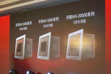
5th Generation KaiXianOn December 28 at a conference dedicated for independently-developed domestic Chinese CPUs, Zhaoxin officially launched their 5th generation KaiXian processors. Fabricated domestically on HLMC's 28nm process based on the WuDaoKou microarchitecture, those processors represent a significant step forward.
Zhaoxin announced two new series based on their latest architecture: KaiXian 5000 (KX-5000) and the KaisHeng 20000 (KH-20000). Note that "KaiXian"/"KX" is exactly the same family as the previously named "Zhaoxin KaiXian"/"ZX". The slight renaming was done to distinguish prior VIA Technologies architecture from Zhaoxin mostly domestically developed architecture.
-
China has the CPU future
This is what happened after China acquired AMD license to produce x64 chips in China, and acquired VIA's x86 license which VIA got from acquiring Cyrix.
The CPU license pool is cracked opened. Soon CPUs in China will be 1/4 the price of Intel/AMD but has better performance.
https://www.reddit.com/r/hardw...
Zhaoxin launched KX-5000 quad/octa-core x86 processors on Dec 28, 2017 in Shanghai, China: image, report, translation.
Zhaoxin revealed KX-6000 & KX-7000 roadmap: image, report, translation.
Other reports: golem.de, pcgameshardware.de, bitsandchips.it, phoronix
KX-5000:
Full SOC design (integrated southbridge)
28nm process by HLMC, 2.1 billion transistors
4-core / 8-core SKUs, no SMT
2.0-2.2GHz base clock, 2.4GHz max turbo
IMC supports dual channel DDR4-2400
PCIe 3.0 lanes
iGPU
integrated audio codec
ZX-200 I/O extension (chipset): SATA3.0, USB 3.1 Gen2, Gigabit Ethernet
OEM: Lenovo desktop M6200KX-6000: 16nm tick-tock
KX-7000: new uArch, DDR5, PCIe 4.0
Related info:
About VIA & Zhaoxin: wikipedia and wikichip.
KX-5000 preview: image, report
KaiXian KX-5000 series was listed in PCI-SIG integrators list on Nov 10, 2017.
Zhaoxin KaiXian KX-5640 in SiSoftware database.
Zhaoxin ZX-C, KX-5000 series on exhibition on Nov 21, 2017 in Ukraine: report, translation.
KX-5000 CPU arch: block diagram, report, translation.
-
Re:Forget Ryzen
More instructions per cycle?
Through the different Core generations they've been refining/tweaking the number of ports and the execution units behind them.don't know what they've done with Coffee lake by skylake/kaby lake is here:
https://en.wikichip.org/wiki/i... -
Re:Intel losing to ARM, not just on mobile
DEC worked with ARM to make StrongARM, then a cross-licensing deal was made between Intel and DEC after a lawsuit.
-
Re:Denormalize
> If it is stupid and it works, it is not stupid.
It depends greatly on the circumstances. Something that works but wastes time is also wasting money.
Schlemiel the Painter's Algorithm for example.
Leaving the paint can in the same spot works, but it's also stupid.
.jpg)
.jpg)
