 Slashdot Mirror
Domain: chip-architect.com
Stories and comments across the archive that link to chip-architect.com.
Comments · 22
-
Re:They Both Fudge
The first gen Conroe Core 2 chips apparently used a similar design trick. It was after all primarily a return to the Pentium III core with a die shrink and some tweaks to support EMT64. Intel was scrambling to recover from the wasteful detour of the Pentium IV. It might have taken them one more gen before the redesign for full 64-bit ALUs - I don't remember anymore.
Well, that link looks like a forum of fanboys rather than a forum of experts (for one thing, they appear to be confusing EM64T, the Intel 64-bit x86 instruction set, with the initial implementations; the ISA is true 64-bit, even if the initial implementations don't have 64-bit data paths, just as an IBM System 360/30 was a 32-bit computer even though it had 8-bit data paths internally and did 32-bit arithmetic a byte at a time).
The first posting linked to an article at chip-architect.com about the 64-bit Pentium 4, and that's the posting that contains the actual analysis of the 64-bit Pentium 4 (as opposed to the shouting on the forum).
About all the forum posters say about Conroe is "seems to apply since conroe as intel fans will tell you KILLS/rapes/pilleges amd in 32bit, but in 64bit they just shrug and ignore the fact that it dosnt perform as well as conroe 32bit perf would emply."; nobody on the forum appears to have actually looked at the die layout as the guy on chip-architect.com did.
-
Re:how many encryption schemes us floating point?
Maybe the FPU shares circuitry with the integer instruction circuitry.
I'm guessing the people modding you +1 funny don't realise that earlier (pre-Prescott) Pentium 4 processors implemented integer multiplication instructions using the floating point unit. -
Re:Heh
Linux Pentium 4 Review
Looking at Intels Prescott -
Take note! Many of these features inside AMD too.
"But Yonah also supports the group of 13 new instructions known as SSE3, handles some SSE2 instructing like Shuffle and Unpack up to 30% faster, and is capable of using its instruction-grouping abilities (known as micro-ops fusion) on some SSE instructions, improving overall throughput."
SSE3 has some very nice hardware thread synchronization instructions. These are important (and AMD has them now). As for the instruction grouping, that sounds rather suspiciously like the double dispatch operations that were added to Opteron:
"Appendix C of Opteron's Optimization Guide specifies to which class each and every instruction belongs. Most 128 bit SSE and SSE2 instructions are implemented as double dispatch instructions. Only those that can not be split into two independent 64 bit operations are handled as Vector Path (Micro Code) instructions. Those SSE2 instructions that operate on only one half of a 128 bit register are implemented as a single (Direct Path) instruction."
Assuming AMD can tune Turion64s to be more power friendly, they'll be able to best Intel's fancy new Core Duo. If they can't, then Intel may be the best game in town for the first time in a decade (assuming they price competitively). -
Re:4MB
The main thing is the overall working set system wide. As long as your TLB has a form of "PID filter," then you don't pay the TLB flush cost across tasks. In that case, you start gaining performance the total working set of the machine fits nicely in the TLB.
Of course, how much of a difference it makes depends on the CPU. As I recall on the Athlon 64s, it has 32 TLB entries at L1 for 4K pages, and 512 entries at L2. (There are actually 40 TLB entries at L1. The remaining 8 are for 2MB/4MB pages.) This works out pretty nicely, as the total working set the 4K pages can cover is 128K at L1 (twice the L1D cache capacity), and 2MB at L2 (between 1x and 4x the L2 cache capacity). Thus, it seems unlikely that a workload that plays well in the cache would play poorly in the TLB.
--Joe -
Re:Some links (from TFA author)
Pentium with an onboard TPM, as this is something Intel has denied.
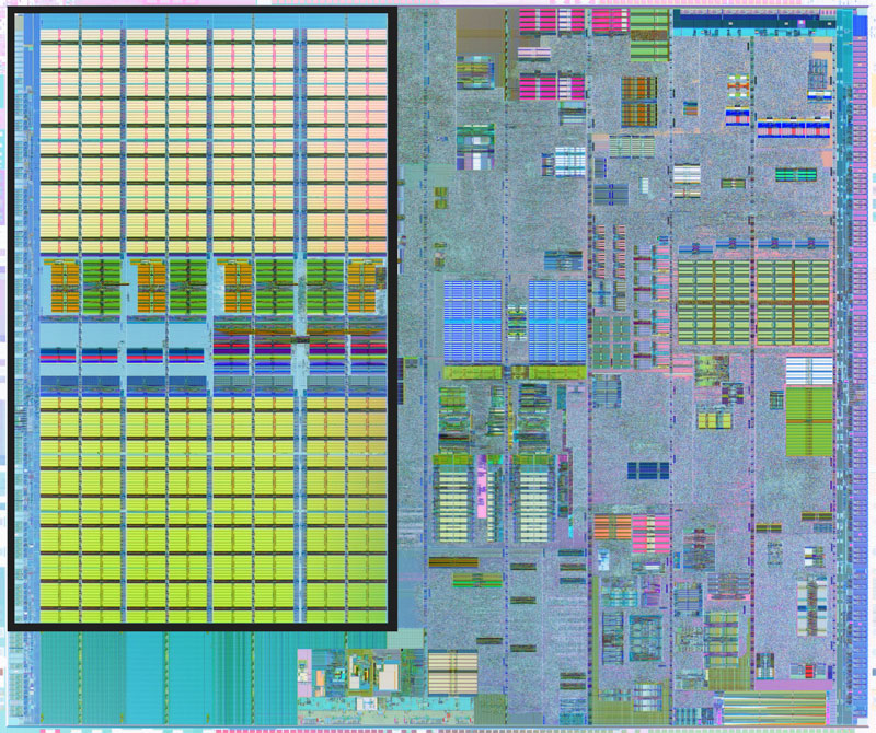
It's apparently inactive: Intel Prescott micrograph, bottom picture on the page.
Richard Clarke's speech about mandatory TNC is here.. I think the date (2001) might be wrong
Yep, 2001. That's the right one. Trusted computing has been in the works for a few years now. The Pentium III CPUID was to be the first step in a step-by-step Trusted Computing deployment, until the backlash.
- -
Re:Who to believe? It's a classic shell game
Intel may also integrate most of the chipset (and the TPM along with it) into the CPU.
You do not need to use the future tense. Intel's CPU-embedded Trust system is codenamed La Grande. If you look at the bottom of this page from TWO AND HALF YEARS AGO you'll find that an inactive version of it is already embedded in the Prescott line and god knows how many other models. If you want to see a more detailed but unlabled micrograph of the chip look here. Note that that this image is rotated 90 to the right compared to the image in the first link I gave. With a little hunting it's not hard to match up the details in the two images, but it's real handy if you have image software to rotate the second image and flip between them.
AMD [] has also jumped on the TCG bandwagon (either that or be run over by it), so it is only a matter of time for them to add a TPM as well.
The AMD CPU-embedded Trust system is codenamed Presidio. AMD has been keeping a tight lid on the project and it took me months just to find the damn name documented anywhere on the 'net.
Cell processor, the TPM is already in the CPU itself,[] IBM claims it is not a full-bore implementation.
Any chance you can elaborate on that? It is well documented that there will be some such system in the Cell, but I haven't been able to pin down any details. In particular, what does "not a full-bore implementation" mean???
- -
Re:SPARC has always been
While the registers visible are limited to 16 in 64bit mode there are way more registers available to the cpu via register renaming. It does add a bunch of transistors but its no longer killing the performance. More AMD64 Info
-
Re:Here comes the flood??
if Intel steps up and builds TCPA support into the CPU itself
From the Inquirer:
Improved architecture for Prescott [CPU] includes better pre-fetcher branch prediction, advanced power management, improvements to hyperthreading technology, the PNI above, La Grande support, better imul latency and additional WC buffers. La Grande is the security feature Intel told us about at the last IDF, and includes protection in the CPU, at the platform level, and with software.
And this story:
Addressing growing security concerns in the PC market, Intel last week also gave a glimpse of La Grande, an on-die technology that will interface with Microsoft's Palladium and other upcoming security software. "We're going to take hardware security up a notch and work with future software developers" to implement the new system, Otellini said. "La Grande is not a Pentium 4 product. It will be a next-generation architecture."
And if you'd like a look at the Trust Chip embedded inside the existing Prescott CPU itself, look to the Micrograph at the bottom of this page. The Trust system eats up about 20% of the CPU die with an entire second CPU and Trust architecture to watch the main CPU.
AMD, Transmeta, and the other CPU makers all have projects to embed the Trust system inside the CPU itself. Oh, and as the recent Slashdot story on the uber-powerful Cell Processor pointed out, it too will have on-chip DRM system. That "DRM system" is doubtless none other than Trusted Computing.
I wouldn't be supprised if motherboard-based Trust chips are pretty much obsolete by the time Microsoft's Longhorn rolls out. (Longhorn a.k.a. Palladium)
- -
Re:Take a deep breath and relax...
it is not going to be running your desktop anytime soon
Wrong.
I have been keeping a list of systems I come accross that are already Trusted-compliant. Note that this is hardly anything like a complete list, it is just the ones I know about:
HP - dc7100 and D530 Desktops
HP/Compaq - nc6000,nc8000,nw8000, nc4010 notebooks (all models)
HP - iPAQ hx2750 Pocket PC
Acer - Veriton 3600GT/7600GT ?5600GT?
IBM - ThinkCenter, ThinkVantage and Netvista desktops, Thinkpad laptops
Toshiba - Tecra M2 Series
Fujitsu - Lifebook S7010 and LifeBook E8000 series
Fujitsu - T4000 Tablet PCs
Samsung - all laptops with "X" in model type
Bestbyte Computers - EXPERT PC 2 System
Link Computers - Ultra P4T-2800
Micaela - Custom Health Care builds
Neutron Computers - Custom build
Neatware - Digital Media Platform and Custom Build
Link Computers - Ultra P4T/PCX PC
One of the PC makers has already committed to making/shipping NOTHING except Trusted complianant systems. I can't swear to which one it was, but I think maybe it was Panasonic?
This one is a bit of a joke, but if the Infinium Phantom Game Console ever actually ships, it's Trusted Compliant as well.
Every major CPU manufacturer is on board with projects to embed a Trust system in CPUs. Intel's codename is La Grande (LG). AMD calls it Secure Execution Mode (SEM). Transmeta's codenameis Transmeta Security eXtensions (TSX). National Semiconductor calls it SafeKeeper or SuperIO. Via Technologies' codename is Padlock.
More codenames:
IBM - ThinkVantage Technology, also known as Embedded Security Subsystem 2.0
HP - ProtectTools
Phoenix - Core Managed Environment
nVidia - ActiveArmor
3COM - Embedded FireWall
I'm not sure of Cisco's codename offhand, but it is part of their Network Admissions Control project (NAC).
Further note that the Trust circutiry is already shipping inside the Intel Prescott CPU, and it eats up about 20% of the CPU die. If you scroll down to teh bottom of this page you can see a Prescott micrograph with the embedded Trust chip outlined in the middle of the CPU. However this Trust circuitry is currenty "inactive" on the chip. I'm not sure if it is physically inert, or if it could be "activated" simply by running the right software.
So your suggestion to "relax" is hardly appropriate. It's rapidly becomeing to late to stop this evil freight train about to run us all over. Trusted Computing is slated to become standard hardware on all new motherboards. It's hard to get an exact timeline on their plans, but I think they expect it to be present in pretty much all new systems by the end of the year.
embedded devices with encrypted onboard flash
You're comparing simple encrypted flash to Trusted computing? That's sort of like comparing a toaster that simply has a foriegn language manual to a pair of handcuffs. Hmmm, More like handcuffs with GPS tracking, chuckle.
But it would take me several paragraphs to get into the details of Trusted Computing. The short version is that the primary design goal of Trusted Computing is to secure the hardware and the entire machine against the owner. When you activate the Trust system you no longer have any control over your computer, you effectly no longer own your computer.
- -
Re:IBM
I don't know what's going on in the Apple universe, but an inactive Trust Chip is already rolled into the Intel Prescott CPU. It eats up about 20% of the chip area.
There is a micrograph of the chip at the bottom of this page. La Grande is Intel's codename for Trusted Computing.
- -
Welcome to Trusted Computing.
As EE Times Reports:
Prescott is also Intel's first processor to support a security technology code-named Le Grande. While Intel has not yet detailed the technology, it is believed to provide a protected space in main memory for a secure execution mode required as part of Palladium, a new PC security scheme being developed by Microsoft Corp.
Le Grande is Intel's codename for Trusted Computing. HP's codename is ProtectTools, Cisco's codename appears to be either NetworkAdmissionControl or SelfDefendingNetwork, Phoenix BIOS code name is CoreManagedEnvironment, and of course we all know Microsoft's codename was Palladium and now is NaGSCaB and is slated to appear in Longhorn.
If you scroll down near the bottom of this page you can catch a look at a micrograph of the Prescott from about a year ago. Note that the Trusted Computing core is it's own an entire CPU and memory and support structures, and eats up about 20% of the chip. In other words Trusted Computing core ties up around 25 million transistors of real-estate, or about half of a Pentium 4.
It will support encrypted code (to secure it against you, the owner), it will encrypt RAM access (again, secure against you) and take over a portion of your cache. It will carry a unique key to identify you and your machine, but far more powerful than the old CPU serial numbers. It will forbid you to know your own encryption keys and prohibit you from decrypting your own data. I know it's designed to work with a "secure clock" (wouldn't want you the owner to be able to "tamper" with the time, now would they?), but I'm not sure if the secure clock is inside the CPU or planned to be external.
AMD has their own Trusted Computing project, but I have been having trouble digging out any hard info. It *may* be incorporated into the Opteron processor.
Transmeta has a trusted Computing project too, the TSX system - Transmeta Security eXtensions. I beleive initially appearing in the Caruso5800.
Welcome to tomorrow. Resistance is futile, all your base already belong to us, Slavery is Freedom, and always remember The Computer Is Your Friend.
- -
64-bit is already in Prescott
Intel seem to have already put necesary element in the prescott die to enable 64-bit computing when they want. At chip-architect they have an article with explaination of the prescott die.
-
Re:saw it comingWell we all saw this one coming with all the delays on the Itanium.
You mean Merced?
We saw this coming with the Yamhill rumors.
And where would we be without stupid pundits?
-
Re:It;'s not that it'll be slower...
As you correctly guess, the Prescott is a VERY major redesign of the P4 core. This article has pictures of both a Prescott and a Northwood die, and they are VERY different (side note: I'm not sure I buy his whole Prescott = 64-bit thing, but the article does have some useful data about the two chips).
In any case, while the power consumption numbers are all over the place, we do have some firm die-size numbers for the Prescott. If you look at Sandpile's P4 page, you can see that the Prescott is listed as having a 112mm^2 die (90nm node) with ~125M transistors. For comparison, the Northwood has a 131mm^2 die (130nm node) with 55M transistors.
A large chunk of the extra transistor budget is going towards the extra cache (the extra 512KB of L2 cache is a good 30M transistors all on it's own), and cache transistors pack in tightly, so the die size/# of transistors ratio ends up being a bit lower than you might expect from just a straight process shrink.
-
Finally Caught On
Chip Architect was speculating on this way back when intel's 64 bit extensions were still called Yamhill. They make some interesting observations that lead them to belive the second 32 bit ALU was to allow for 64 bit integer operations in a 2x32 bit format. And not to assist with eliminating resource shortages in HT as some others had suggested.
And even if that does pan out it's highly unlikley to appear in desktop Prescott core chips anytime soon. Seems much more like something you'd find in Xeon MPs and later DPs to eliminate the need for that hack they call PAE.
Though i hardly see how 'somebody told us a seinor exec said' makes Slashdot.' (I understand that's what the Inquirier bases most of their news on, i thought we had slightly higher standards of reliability) -
Re:Great for consumers
Intel have been sampling their 90nm parts to various OEMs around the world for about six months now. Believe me, they're about to up the ante. See this website if you want to learn a bit more about the 90nm Pentium 4.
-
Re:Electro-Magnetic Headache.
Running at 5-7GHz is absolutely retarded for a processor to do.
A big chunk of the Pentium 4 already runs at twice the rated clock rate. In other words, there are parts of the P4-2.4GHz on my desktop that are running at 4.8Ghz.
There is some speculation on the net that Intel is basically going to start using this higher clock rate as the clock speed in their marketing literature. The idea is that enhancements to the hyper-threading technology to be released in Prescott will give a significant enough jump in performance to allow the marketing people to justify the sudden x2 in published clock rate.
There is a lot of speculation and analysis done at this site http://www.chip-architect.com/.
As a side note, they also speak towards how next generation these chips might run 64-bit code, a la x86-64. Apparantly, there's reason to believe that the Prescott die has ALU's and support for 64-bit x86 code already on board. Nothing is said about piggybacking a second chip... -
Finally caught on?
Chip Architect was speculating on this way back when intel's 64 bit extensions were still called Yamhill. They make some interesting observations that lead them to belive the second 32 bit ALU was to allow for 64 bit integer operations in a 2x32 bit format. And not to assist with eliminating resource shortages in HT as some others had suggested.
And even if that does pan out it's highly unlikley to appear in desktop Prescott core chips anytime soon. Seems much more like something you'd find in Xeon MPs and later DPs to eliminate the need for that hack they call PAE.
Though i hardly see how 'somebody told us a seinor exec said' makes Slashdot.' (I understand that's what the Inquirier bases most of their news on, i thought we had slightly higher standards of reliability) -
Regarding K8/Hammer performance features
> the Hammer/x86-64 chips have ondie memory controllers AND more registers than i386++ type
> chips, combined they'll give a speed increase of not inconsiderable proportions.
It is notable to, er, note that the former advantage helps (possibly considerably) towards both recoded AND legacy (eg, normal) programs, whereas the additional physical registers would require recompilation in order to show a benefit, which means that everybody but Windows users will get an immediate use outta that.
Other advantages of the Hammer? Well, not counting the 64-bit yunk (that WILL provide benefits, but I want to cover benefits that will help legacy programs, like Civilization III, The Sims, Unreal II and other antiproductivity applications):
Hyper Transport. That's not much on its own, but it essentially equates to a reduction in loss of bandwidth to the chipset and between processors when you add an additional processor. On the Intel setups, the processors share a set amount of bandwidth to the chipset, so putting eight chips on a 2.4GB/s bus means that you have each chip getting 0.3GB/s. The AMD setup theoretically lets each processor get that 2.4GB/s. Of course, that's in a perfect world, chip-level, but it probably amounts to some benefit. AMD's K7 family has similar advantages, which probably assists in explaining why they get higher performance at each given clock in mainstream applications (which at least somewhat depend on the memory subsystem) even though the AMD cpu to memory bandwidth was usually 2.13GB/s (now it's 2.67GB/s, unless you count stuff like the nForce, which has some extra memory bandwidth, but the extra benefit there is eaten up by the onboard video), whereas the Intel cpu to memory bandwidth was usually 3.2GB/s. Anyway, the idea is that HyperTransport will (on a hypothetical level) make it much easier to make n-way systems without either a tremendous performance impact or an expensive crossbar workaround setup thingy.
SoI. Silicon-on-Insulator. This is one of those things that'll help with the process technology. In the end, it'll probably offer a little bit of a frequency boost by making the chip a little cooler or something like that. I forgot precisely what SoI's primary benefits were. It's been months since I've even thought about it.
Stages: As detailed here, the K8 adds two stages to the decoding part of the instruction pipe. The decoding part of the pipe is probably rather complex, so you may see a pretty neat frequency boost over the K7 family without the problem of a huge branch mispredict penalty. The number of cycles that a cpu wastes when it makes an incorrect guess on a low level "if/then" statement is somewhat proportionate to the number of pipeline stages. The AMD K6 and (iirc) Cyrix 6x86 were the mack daddies of branch prediction, since their pipes had only five stages or so, so they only had to wait a few cycles when they zigged instead of zagged. The PIII and K7 had over ten stages, so they had to wait a lot longer, but other advantages (such as the larger and sometimes faster caches and more accurate predictors) in those processors over their predecessors did their best to overcome this disadvantage. The Pentium 4 has a crippling 20 to 28 (depending on the situation, and depending how the trace cache handles the situation, and whether or not you want to count it) stages. This means that it can hit amazing clock frequencies, but it'll get cranky and drowsy for twice as long when it makes a predictive mistake. How does it get away with this? Well, the trace cache does its best to assist, but it didn't really help as much as I think the designers were hoping. But for multithreaded programs and OSes, the SMT implementation on the more recent members of the P4 family, an implementation known as "Hyper-Threading", probably pretty neatly alleviates much of this problem by putting operations from other threads into the cpu whenever the currently running thread stalls on a branch mispredict. The K8/Hammer approach is just to add stages where they hopefully will have the most balanced, beneficial effect to frequency boosting while only minimally increasing the branch penalty. SMT would be nice, but it isn't nearly as critical a need as it is on the P4.
Wider memory access. On the Sledge Hammer, if AMD's plans are still the same as when I wrote this, the memory controller (which is embedded onto the cpu) will access PC2700 memory in a 128-bit configuration (ignore the "126-bit" typo on the linked page -- I can't believe I didn't notice that when I typed it nearly a year ago!), which leads to a 5.3GB/s path to memory. That's damned good, though I really think AMD should have focused on 366/183MHz (equiv to "PC2933") or 400/200MHz (equiv to "PC3200") memory instead of the 333/166MHz PC2700 that came out over a year ago. Still, servers often use memory that's lower than bleeding edge clock in order to maintain reliability, so bleh. Still, 5.3GB/s isn't bad for a setup that isn't based on a shared bus.
Enhanced branch predictor. Well, that's if my notes from a year ago are accurate. If true, this'll probably overcome any mispredict penaly performance disadvantage from those abovementioned added stages.
Larger TLBs, TLB flush filter, etc.. This stuff will have itty bitty advantages on a per-clock performance basis, but every little bit helps.
Larger caches. Hey, I should look this up to see what they're planning on. Is it just 512KB on-die L2, or is AMD planning on bringing it up to 1MB L2? The interesting thing about AMD's designs is that the die is really small on each processor. Remember how AMD has gotten occasional fire for processors overheating? Well, aside from a stupid lack of shutdown diodes in the past, the real cause wasn't that the AMD processors used more heat than the Intel processors. They usually generated about the same amount of heat, often less, but their processor surface area was substantially smaller, which made the chips less expensive to produce and less likely to have defects. But when you try to push an equal amount of heat through half the surface area, you end up with a higher amount of heat per area, which equates to a higher running temperature. The funky thing about this is that you could just added a whopping huge amount of on-die cache. That'd increase performance while also increasing the surface area. But the heat production would not be substantially affected. So you'd end up with a lower temperature processor. So the Hammer will have a higher ratio of cache to processor units in the cpu, so it won't be as much of a fire hazard. Frankly, they should have put 1MB on-die L2 onto the Thoroughbred/AthlonXP.
Crap. I need to research more on the K8. It probably changed a lot since I went into hibernation. The interesting thing is that in the last half year, I've largely moved from being a Windows 2000 power user to a Linux coder (I still use both operating systems for several different purposes, but I'm talking primary usage). I stand to be in the group that benefits most from the Hammer when it comes out, since I'll be able to './configure && make' or 'qmake -project && qmake && make' most of the programs I use and/or develop. So I'll instantly see the benefit of those extra registers. ^_^
-JC
http://www.jc-news.com/ -
Working on an architecture that does this...
I'm involved in a project involving a SMT (well, more CMT) processor design. We do not yet have any silicon, but are getting good results in simulation.
We have a simulator that can be set to simulate a processor with any number of closely coupled cores, and any number of threads per core. We get good results at a 8 core * 4 threads setup (total up to 32 way parallel).
Using some basic automatic parallelization on a piece of code designed to run in a single thread, we have generated up to a 26X speedup, 8 core * 4 threads versus 1 core * 1 thread.
The advantage of SMT over a normal processor is that it makes use of clock cycles that would otherwise be wasted, eg waiting for the cache to fill. If your architchture spends half of its time stalled, and you can make use of these cycles by adding SMT, then you can increase your processor performance very efficiently.
SMT basically requires you to duplicate all of the processor's registers n times (n = #threads), + a little extra hardware ('little', relative to duplicating the entire core). So for ((1 * core) + (2 * registers) + SMT hardware) you are getting the performance of ((2 * core) + (2 * registers)). Good bang per buck ratio, when you count up the transistors.
But SMT naturally gives you diminishing returns for each thread you add - the whole point is that each new thread is using up wasted cycles - and once you reach ~4 threads there are very few cycles left over. At this point, if you have room left over on the die, you may as well start thinking about SMP on the same die.
Surpriesd the article didn't mention SMT & AMD. Check out this link.
-
Re:You have way too much time on your hands, frien
First off, apologies for slipping in ad hominem attacks in my post. However, this was just in response to your similarly inappropriate attacks on Johan and Ace's. The difference, of course, is that my comments were in support of the correct analysis, not disparaging it.
This is not a site on which every little review and rant is meant to be posted. Hannibal's article belonged here because, well, Hannibal is an expert on the technology behind microprocessors.
1) It was Hemos' decision to post this; anyone can submit anything they deem worthwhile.
2) This was neither review or rant, but rather a lengthy and insightful look at some subtle but very important issues that will influence P4 vs. Mustang performance. Just because you've never seen anything on the web supportive of the P4 doesn't make a balanced piece a rant; it just means that you've been reading a lot of ignorant writing.
3) Humorously enough, the "self-promot ing" Hannibal link I offered was exactly "every little review", this time of some gimmicky portable (but monitor-less) PC. I found it entertaining, and was happy to see it on
4) Hannibal is NOT an MPU expert. He himself will acknowlege this, and has in his articles (don't have time to find where). Email him yourself and ask him who is more of an expert, himself or Johan De Gelas, and I am relatively certain he'll say Johan. If not, he will readily admit that Johan is at least his equal and that Ace's is a much more technical site than Ars. And he will most certainly admit that Paul DeMone is 10 times the expert he is. Again, I really really like Hannibal's work, it honestly inspired me, and I submit every new Hannibal-on-architecture article to
And, just FYI, I have read every single article on microproccessor design that has passed by the
ROFLMAO!
You read the scant handful of poorly chosen architecture articles linked from slashdot and you consider yourself an expert??? HAHAHAHAHAHA. Oh--and sometimes you check your facts with little old 16-year old Anand.
Look dude, it isn't my place to criticize you for not knowing as much about MPU design as I do. It is my place to criticize you for not realizing that there is much more to be known, for not realizing that many people do know more about it than you. I am certainly no expert--I'm just a college student--but it is blindingly clear that I know more about it than you, just as it is clear to most
Second it's quite clear that you essentially skipped all the parts of the article you didn't understand and concluded that if you--with your expert education on MPU design from
No, Johan didn't take what might be called the "Hannibal route"--i.e. launch into an exploration of the overall design philosophies behind the two cores--because he is writing for a specific audience, a knowledgeable technical audience who can be expected to have read several pieces explaining the important design features of the P4 (not much concrete is known about the Mustang other than that it will be a K7 with tweaked layout to improve critical path and power consumption, and that it may recieve several other enhancements as speculated in the article), specifically those here, here, here, here, and here. Not only have most regular readers of Ace's read all these articles, but they have followed some very interesting debates on them between industry experts on the Ace's tech forum for months now. It might be fair to criticize Johan for submitting an article which clearly assumed such a technical background to
Re: preproduction benchmarks, the Tom's piece on the PII and the Firingsquad piece on the K7 were generally the only benchmarks available of the respective chips before their launch. If you followed MPU design news as closely as I do you would know this. There is a thing called an NDA, after all; as these two pieces demonstrate, both Intel and AMD like to make sure that those who choose to break theirs post erroneous information.
You're of course right that a PPro was indeed superior to a PII at a given clock speed; if you look through the article itself instead of just relying on the concluding quotes I posted, you would find benchmarks which clearly understate the known performance of the PII by as much as 30 or 40%, though. There is no doubt Tom's preproduction benchmarks, like Firingsquad's, were horribly off. And as long as you're disputing my "always" contention--I've ponied up the links (and no, it didn't take me very long at all, because I, having followed MPU developments for a couple years, knew for example that it was FS with the bad preproduction K7 benchmarks, and Tom with the PII controversy); why don't you post a single pre-NDA "review" or even just a series of leaked benchmarks on a new x86 core which proved entirely accurate?
Re: definition of a 7th-gen core: You really should pay more attention in class, boy, because I'm schooling you right now. I explained what I meant right after that comment in the original post: The Athlon is a new core designed to scale well to very high clockspeeds. Just like the Willammette. That's why the Willamette performs slower clock-for-clock than a theoreticl P!!! at the same clockspeed
First off, there is no evidence that the P4 has lower IPC than the P3, except for preproduction benchmarks and some ambiguous comments from Intel VPs. If you read my previous post at all, you would realize these would tend to indicate that the P4 actually has higher IPC, not lower. On the other hand, the main evidence that it has higher IPC is that an analysis of all the new, innovative, braniac features of the core strongly indicate that it must.
And second off, you couldn't be more wrong. By calling the K7 a "7th-gen core" you are obviously comparing it to the 6 previous generations of Intel cores. Each of them was able to improve both clock speed on identical process and IPC significantly over the previous generation. The Athlon beats the P6 in clock speed on identical process...but only narrowly: the Athlon sweet spot right now is around 1 GHz on Dresden's
Meanwhile, P4 roadmaps indicate that it will scale 100% better than the P6 on identical processes, and the analysis of Paul DeMone, a far greater MPU expert than you or I could hope to be, is that it will have 15-20% better IPC for integer work, and considerably greater gains for FP. (It's too soon to tell without knowing more about how well compilers will optimize for SSE2.) That would be a 7th-gen core worthy of the leap from 5th to 6th which the P6 provided.
Again, don't get me wrong: the Athlon is clearly clearly superior to the Coppermine P3. But only by about the same degree as the Coppermine P3 was superior to the Katmai P3. That is, *not* by a full "generation"--whatever the hell that is.
Re: important innovations in the K7: It's a huge innovation in the x86 world, something Intel hasn't done since the PPro days. First of all, the EV6 bus is new to x86 and a huge innovation, it is superior in every way to the old Intel GTL+.
BWAA HAA HAA HAA HAA HAA!! Man, I'm rolling on the floor and crying that's so pitiful.
Oh, but I'm being rude. Ahem. Pardon me. You, uh...you do know why it's called the EV6 bus, don't you?
HAA HAA HAA HAA HAA! I asked you to pick one innovative feature of the K7, and you picked the one feature that AMD DIDN'T INVENT!!!!!
Ok, I'm over it now. Phew.
Right. AMD didn't invent the EV6 bus. They didn't help develop it. They in fact had nothing to do with it. They licensed it, wholesale, lock, stock, barrel, from Compaq where it has been in use for quite some time now. On the one hand, it was a good business decision because Intel had just clamped down and decided not to relicense the P6 bus (not really called GTL+ BTW, but don't worry it's a very common mistake) to AMD, and rather than take the time to reinvent the wheel (and thus delay the launch of the K7), AMD decided to go shopping at Compaq. Fine. Smart decision.
Don't give me any of this revisionist history that they did it because it's 200 MHz, though. The K7's extra FSB bandwidth (courtesy of the EV6 bus (and the engineers at Compaq, not AMD)) has up till now been entirely wasted as it is paired with SDR SDRAM (1.6 GB/s FSB, only 1.06 GB/s from DRAM)--generally paired asynchronously with PC133. If it were any help at all, don't you think the Athlon would be winning and not losing in FSB-intensive benchmarks like Q3? Meanwhile, it's a huge waste of pins and power--as well it should be, since it was originally designed for $10,000-50,000 workstations and servers, which, frankly, can afford the extra mobo costs, power supplies and electric bills.
Now, of course this extra FSB bandwidth will finally be put to good use with the advent of DDR mobos for the K7, *finally* starting early next month (fingers crossed!); latest news is the 1st. DDR mobos for the P3 will show less improvement because the P3 is stuck at 133 MHz FSB. Fine.
But this isn't why AMD chose the EV6. Indeed, when they made that decision, the DDR standard had either barely-just-been or had-not-yet-been determined by JEDEC. Intel was set to steamroll RDRAM into every PC, and there was little to no indictation that DDR would ever be a volume part in the PC industry. (It'd be used in servers and such.) AMD chose the EV6 because they *had* to, not because they wanted to. It's a great bus when doing what it's designed for--connecting specially made (quite expensive) double-wide SDRAM to Alphas, at FSB freqencies up to 466 MHz. But it offers little to no performance benefit in the here and now for the K7. And as for DDR and high-speed buses, Intel will be releasing their Tualatin revision P3's in Q2 with a 200 MHz FSB, in time for Almador, their (maybe--legal issues with Rambus...) DDR P3 chipset. So yes, the K7 will be first with decent DDR support in the x86 space. The P4's dual-RDRAM chipset and 3.2 GB/s FSB will be faster, though more expensive, as far as memory performance goes, though.
But calling a bus that AMD had exactly zero nada zilch nothing to do with evidence of their design innovation gets an extra HAHAHAHAHAHA from me.
More on AMD's innovative EV6 bus: it's a huge boon for multiprocessing, with the 760MP coming to retail very soon according to Anand.
Unfortunately, according to AMD's Q3 earnings report Investor Conference Call 2 weeks ago (I was listening; somehow I doubt you were...), the 760 MP has been delayed to at least Q1, possibly Q2. They played it off as strategic reasons (business demand down; no major deals with the big 4 server OEMs (Dell, IBM, HP, Compaq) for AMD in the enterprise lines), but considering they only had one 2-way system--behind closed doors and not running anything--at MPF it looks as if their engineering is behind too. On the one hand, too bad, because point-to-point beats shared bus any day. On the other, there's a reason why Intel went with shared bus, and it's not because they'd never heard of PTP. It's, well, easier to implement. When doing the right thing takes over a year longer, it sometimes becomes doing the wrong thing. (Not that I believe that's true here, but it's worth taking into consideration.)
Now, the countryside is littered with Athlon clusters crunching numbers for the scientific community in places where they'd never have considered using a P!!!.
First off, scientific computing is such a niche market as to have absolutely negligable impact on the bottom line of either company. The idea that AMD designed the K7's huge-ass FPU--thus taking up vital die-space--for the lucrative physicist market is laughable. It's an unbalanced design, plain and simple. Second, last time I checked, most scientific computing was being done either on Alphas or on Beowulf's of Celerons. Now, I don't doubt that K7's are moving heavily into the mix; if I was doing scientific computing, I would go with a cluster of Durons in a heartbeat.
But do you really, honestly, think that when AMD decided to go with the 3-wide FPU there were dreams of meteorology and electron potential modeling spinning in their heads? Me either.
And your "analysis" of the supposed advantages of the Coppermine's cache over the Thunderbird's are positively laughable. You see, in the REAL WORLD people don't run benchmarks on their boxes all day. They run apps and processes, usually several at a time. That's why the Athlon's cache is superior--you can keep more in it instead of swapping to system RAM, which is a MUCH BIGGER HIT than having a small amount of cache latency. In the REAL WORLD, the Athlon's cache architecture makes sense, not in your fantasy where we all run CPUmark all day.
Uhhuh. That's why the Katmai P3--with its half-speed 512 Kb L2--was so much faster than the Coppermine? That's why the Athlon "Classic"--with down to 1/3-speed 512Kb L2--is so much better than TBird??
You think it's faster to perform a context switch with a 64-bit bus to L2 than a 256-bit one? Golly, imagine how slow the P4 with its 48 GB/s bus to the 5-cycle latency L2 will be!!
Furthermore, in case you'd forgotten, all these chips operate at over one billion cycles per second. Multitasking occurs at much higher granularity than this, and even if your analysis were right (it's not), the effects of multitasking are invisible to a chip to a second or third order of approximation. The effects of a 7 (or 5!) cycle L2 vs. an 11 cycle one most certainly are not.
And then you go on to say that the K8 will just be a derivative of the K7. You really aren't paying attention at all. The K8 Hammer architecture is completely new, not only extending x86 to true 64-bit while retaining backwards-compatibility with 32-bit and 16-bit code, but adding huge and significant architectural innovations. Go read about it, dimwit, before you guess at what it is. Lots of documentation has been released--even just a quick scan of some Slashdot search results will make you a lot more knowledgeable about it than you are now. Geez...
No, this is false. It is by now quite well known that what will define the Hammer family will be just a simple extension of the x86 ISA to 64 bits--an extension which will have essentially no use for the average PC user, but rather only for those who need 64-bit integer precision (CAD, etc.) or >32-bit memory address space (database, etc.). In addition, "the K8"--that is, the Sledgehammer, aimed at the enterprise market--will feature 2-way CMP and AMD's new Southbridge standard, LDT. Ho-hum. Nice features (LDT has no place in the PC either, though), but nothing extraordinary, especially considering it's not due until early 2002. In addition, there has been mention (Sanders mentioned it in an interview) of another K8 variant called Clawhammer; speculation is that this is a PC version of the K8, although it's not known what, other than x86-64, will differentiate it from, say, Palomino.
If you actually believe the K8 represents an entirely new design, then it may be that your news was correct but just a little (about 12 months) late. The K8 was indeed scheduled to be a ground-up clean-sheet kick-butt design, but was radically scaled back by Sanders less than a year ago. Head Designer and impressive guy Atiq Raza quit around a year ago, following this decision, and the hopes of a truly innovative K8 went with him. Of course, evolution is often better than revolution in the MPU industry--eg. RDRAM. If it can manage to position itself against Itanium, the K8 might look very strong. (Of course, McKinley will be on the way by then, and it's considerably less of a joke.) But claiming that the K8 is a revolutionary new design is plain false.
As for the recent
Re: P4 moving into heavy volume in Q3 2001: God, you are a shameless, and dim-witted, Intel apologist, just as I suspected. Q3 2001?
How precisely does this make me an Intel apologist? Is it too early?? It is a known fact that Intel's roadmap moves the P4 solidly into the mainstream category in Q3 '01 with the introduction of the Northwood P4 on a
Is it too late?? The latest Intel roadmap shows the P4 moving to the upper end of the mainstream category in Q2, but I believe that to be a lie by Intel marketing, eager to cover up the fact that they essentially have no upper-mainstream product from now until Q3 2001, a hole in their product line a mile wide. (Am I still an Intel apologist?) Indeed, this is the reason I just bought AMD stock very recently, and have been encouraging my INTC-owning relatives to sell ever since, well as it turned out, just before the peak late this summer. And yes, like you too I am generally appalled by Intel's heavy-handed anti-consumer tactics--suing VIA and refusing to release a PC133 chipset in a lame attempt to force RDRAM down the industry's throat; paper launching the 1 GHz P3 6 months before even limited volume was available, the 700-850 MHz P3's before it around 3 months early, and the 1.13...oh the 1.13...all in a lame attempt to pretend the P6 could keep up with the Athlon; bribing Michael Dell with special pricing and all several dozen GHz P3s available this summer to spread libelous statements to the media in a lame attempt to disparage AMD's products; spreading IA-64 FUD in a lame though successful attempt to scare designers of competing RISC chips to delay (Compaq, HP) or eliminate (MIPS) their next-gen chips; keeping the Celeron FSB clocked at 66 MHz and "single-processor only" in a lame attempt to...be lame.
Don't worry, I dislike Intel plenty a lot. I cheer for AMD, and make no bones about it.
What bothers me, though, is that, having been on the Athlon bandwagon since summer 1999, when I first read analyses of how the K6's poor scaling was due to architecture not process quality, and how the better balanced K7 had the chance to scale even higher than the P3, I've seen how this position has gone from being contrarian, well-informed and far-sighted to the position of a growing mainstream of ill-informed buzzword-spouting reality-ignoring AMD fanboys. No, not you; the people I'm talking about are much much worse (and hence not nearly as able to fool
Plus, AMD's execution with the K7, while quite good, has been well short of the claims that I and many others were making for it over the past year. The benchmarks have been disappointing. There's only so much excitement you can get out of awesome benches in 3DSMax and ViewPerf before you notice those Q3 and Content Creation scores just aren't going to change. (Yes, I know CC is Intel-biased. Whatever.) Thunderbird in particular was a huge disappointment, offering gains on the order of 3-5% over Athlon Classic while the Coppermine P3 beat Katmai by 10-15% (it's that 64-bit vs. 256 bit L2 bus). MP has been MIA for months now. The K7 laptops are late as well; high power-consumption is the price you pay for unneeded FPUs.
Having read the Willamette articles I've now referred you to twice (the DeMone ones on RWT), having seen Paul defend his unorthodox position on the Ace's tech boards for months now, basically skewering even very well-informed arguments on the AMD side, I've gradually become convinced that the "web hardware community" is greatly underestimating the P4's performance. So have many people much more knowledgeable than me--including the formerly (and still, though less so, IMO) AMD-biased Johan.
I usually go around looking to argue with P4-bashers who seem intelligent and well-versed in the technology, because they give the most interesting arguments and are the most willing to learn. Unfortunately, I too often have to correct well-meaning but misleading posters like yourself, who ignorantly pass on the same-old wishful thinking and oversimple analysis as fact.
I like AMD. I really do. I want them to "win", inasmuch as I want anyone to. I really do want them to stay very very competitive, like they are now. (And to make me lots of money!) But I just don't think it's helping them, or helping the truth, to pretend that the K7, a largely derivative design, will be able to keep up with the radically innovative P4 for very long. And I don't think it's furthering the principles of beauty and elegence in design--which is what really interests me in this stuff anyways--to call an insightful and fair (I thought it strongly gave AMD the benefit of the doubt, BTW) analysis of the strengths and weaknesses of the P4 and Mustang designs "an ignorant fluffy rant", or whatever you said.
I won't expect the apology from you, but you have my email address if you should want to send it. Meanwhile, if you're really interested in MPU design, please read Paul's articles at RWT; they're fabulous and take everything to a whole new level. And if they must be anti-Intel, you can't do better than his Merced/Itanium articles, here, here, here and here.
Also you should check out the tech forum at Ace's, and the very AMD-biased but usually literate and often a great site for news and links...JC's. Plus the usual suspects: Tom's, Ars, The Register for juicy-and-occasionally-even-true rumors. You could learn a lot, and trust me, it's fascinating stuff.